
 english
 chinese
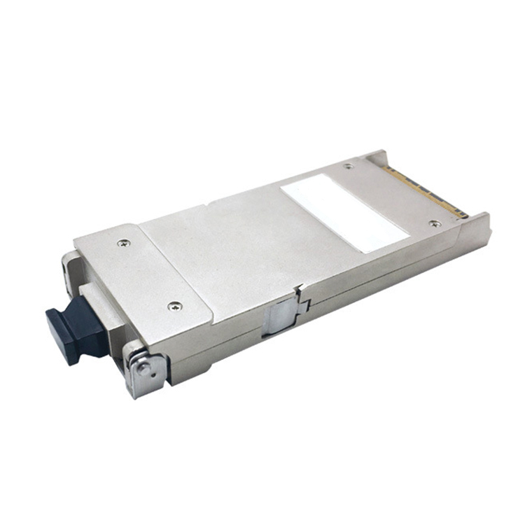
Your Position : home >Products > Fiber Optic Active Devices > Optical Transceiver > 100G Optical Transceiver
Products
-
5G System
- Fiber Optic Cable System
- Fiber Cable Distribution System
- FTTH System
-
Patch Cord Production Line
- Fiber Stripping Machine
- Cable Stripping Machine
- Fiber Optic Cutting Machine
- Fiber Optic Polishing Machine
- Fiber Optic Polishing Fixture
- Fiber Optic Heating Oven
- Fiber Optic Crimping Machine
- Fiber Optic Epoxy Injection Machine
- Fiber Optic Microscope
- Pre-Assembly Tools
- IL&RL Testing Machine
- Ultro-sonic cleaning machine
- Interferometer Testing Machine
- Polishing Consumables
- Fiber Stripping Machine
- Fiber Optic Active Devices
-
Optical Cable Pulling machine
<
>
100Gb / s 10KM CFP2 Optical Transceiver
Application:
1.OTN-OTU4
2.Switch to switch interface
3.Switch to router interface
4.P to P Access Network
2.Switch to switch interface
3.Switch to router interface
4.P to P Access Network
Characteristics:
1.Direct LC receptacle optical interface
2.Single +3.3V power supply
3.Hot-pluggable
4.Operating optical data rate up to 112Gbps
5.Operating electrical serial data rate up to 10.3125Gbps
6.10 parallel electrical serial interface
7.Transmission distance up to 10km
8.AC coupling of CML signals
9.1310 nm window cooled EA-DFB LD
10.PIN ROSA
11.Low power dissipation(Max:16W)
12.Built in digital diagnostic function
13.Operating case temperature range:0℃ to 70℃
14.Compliant with RoHS
15.MDIO Communication Interface
Ordering Information
| Part Number | Product Description |
| FYCP2-4LO4-10BD | CFP2: 1310nm-LAN-Cooled-EMA DFB-LD, 103.125Gbps, 10km, 0?C ~ +70?C, Ethernet Version, DDM |
Absolute Maximum Ratings
| Parameter | Symbol | Min | Max |
| Storage Temperature Range(℃) | Ts | -40 | +85 |
| Relative Humidity(%) | RH | 5 | 85 |
| Power Supply Voltage(V) | Vcc | -0.5 | +3.6 |
| Operating Case Temperature Range(℃) | Tc | -5 | +75 |
| Receiver Damage Threshold Per Lane(dBm) | Pdag | +5.5 | - |
Recommended Operating Conditions
| Parameter | Symbol | Min | Typ | Max |
| Operating Case Temperature Range(℃) | Tc | 0 |
|
70 |
| Power Supply Voltage(V) | Vcc | 3.2 | 3.3 | 3.4 |
| Data rate(Gb/s) |
|
|
103.125 | 112 |
Specifications (tested under recommended operating conditions, unless otherwise noted)
| Parameter | Symbol | Min | Typ | Max | Notes | |
| Voltage Supply Electrical Characteristics | ||||||
| Supply Current(A) | Tx Section | Icc | - | - | 3.5 | 1 |
| Rx Section | ||||||
| Power Supply Noise | Vrip |
|
|
2% | DC-1MHz | |
|
|
|
3% | 1-10MHz | |||
| Dissipation(W) | Class5 | Pw |
|
|
12 |
|
| Low Power Dissipation(W) | Plow |
|
|
2 |
|
|
| Inrush Current(mA/usec) | Class5 | I-inrush |
|
|
200 |
|
| Turn-off Current(mA/usec) | I-turnoff | -200 |
|
|
|
|
| Different Signal Electrical Characteristics | ||||||
| Single Ended Data Input Swing(mV) |
|
55 | - | 525 |
|
|
| Single Ended Data Output Swing(mV) |
|
150 | - | 500 |
|
|
| Differential Signal Output Resistance(Ω) |
|
80 |
|
120 |
|
|
| Differential Signal Input Resistance(Ω) |
|
80 |
|
120 |
|
|
| 3.3V LVCMOS Electrical Characteristics) | ||||||
| Input High Voltage(V) | 3.3VIH | 2.0 | - | Vcc+0.3 |
|
|
| Input Low Voltage(V) | 3.3VIH | -0.3 | - | 0.8 |
|
|
| Input Leakage Current(uA) | 3.3IIN | -10 | - | +10 |
|
|
| Output High Voltage (IOH=100uA)(V) | 3.3VOH | Vcc-0.2 | - | - |
|
|
| Output Low Voltage (IOL=100uA)(V) | 3.3VOH |
|
- | 0.2 |
|
|
| Minimum Pulse Width of Control Pin Signal(us) | t_CNTL | 100 |
|
|
|
|
| 1.2V LVCMOS Electrical Characteristics | ||||||
| Input High Voltage(V) | 1.2VIH | 0.84 |
|
1.5 |
|
|
| Input Low Voltage(V) | 1.2VIL | -0.3 |
|
0.36 |
|
|
| Input Leakage Current(uA) | 1.2IIN | -100 |
|
+100 |
|
|
| Output High Voltage(V) | 1.2VOH | 1.0 |
|
1.5 |
|
|
| Output High Current(mA) | 1.2IOH |
|
|
-4 |
|
|
| Output Low Current(mA) | 1.2IOL | +4 |
|
|
|
|
| Input Capacitance(pF) | Ci | +4 |
|
10 |
|
|
| Optical transmitter Characteristics | ||||||
| Signaling Rate for Each Lane(100GbE)(Gbps) |
|
- | 25.78125 |
|
|
|
| Signaling Rate for Each Lane(OTU4)(Gbps) |
|
- | 27.95249 |
|
|
|
| Four Lane Wavelength Range(nm) | λ1 | 1294.53 | 1295.56 | 1296.59 |
|
|
| λ2 | 1299.02 | 1300.05 | 1301.09 |
|
||
| λ3 | 1303.54 | 1304.58 | 1305.63 |
|
||
| λ4 | 1308.09 | 1308.09 | 1310.19 |
|
||
| Side Mode Suppression Ratio(dB) | SMSR | 30 |
|
- |
|
|
| Total Average Launch Power(dBm) | Pt | - |
|
10.5 |
|
|
| Average Launch Power for Each Lane(100GbE)(dBm) | Pa | -4.3 |
|
+4.5 | 2 | |
| Average Launch Power for Each Lane(OTU4)(dBm) | -2.9 |
|
+4.5 |
|
||
| Optical Modulation Amplitude for Each Lane(dBm) | OMA | -1.3 |
|
4.5 | 3 | |
| Transmitter and Dispersion Penalty for Each Lanes(TDP) |
|
|
|
2.2 |
|
|
| Extinction Ratio (100GbE)(dB) | EX | 4 |
|
|
|
|
| Extinction Ratio (OTU4)(dB) | 7 |
|
|
|
||
| RIN20OMA(dB/Hz) |
|
|
|
-130 |
|
|
| Optical Return Loss Tolerance(dB) |
|
|
|
20 |
|
|
| Transmitter Reflectance(dB) |
|
|
|
-12 |
|
|
| Eye Diagram | Compliant with IEEE 802.3ba-LR4/OTU4 | |||||
| Optical receiver Characteristics | ||||||
| Signaling Rate for Each Lane(100GbE)(Gbps) |
|
- | 25.78125 |
|
|
|
| Signaling Rate for Each Lane(OTU4)(Gbps) |
|
- | 27.95249 |
|
|
|
| Four Lane Wavelength Range(nm) | λ1 | 1294.53 | 1295.56 | 1296.59 |
|
|
| λ2 | 1299.02 | 1300.05 | 1301.09 |
|
||
| λ3 | 1303.54 | 1304.58 | 1305.63 |
|
||
| λ4 | 1308.09 | 1308.09 | 1310.19 |
|
||
| Overload Input Optical Power(dBm) | Pmax | 5.5 |
|
|
5 | |
| Average Receive Power for Each Lane(100GE)(dBm) | Pa | -10.6 |
|
4.5 | 6&7 | |
| Average Receive Power for Each Lane(OTU4 with Tx ER of 4 to 6.5 dB)(dBm) | Pa | -6.9 |
|
4.0 |
|
|
| Average Receive Power for Each Lane(OTU4 with Tx ER > 7 dB) |
|
-8.8 |
|
2.9 |
|
|
| Receive Power In OMA for Each Lane(dBm) | PinOMA | - |
|
4.5 |
|
|
| Difference in Receive Power between Any Two Lanes(dBm) |
|
- |
|
5.5 |
|
|
| Receiver Sensitivity in OMA for Each Lane(100GbE) at BER= 1x10^–12(dBm) | SOMA | - |
|
-8.6 | 8 | |
| Equivalent receiver sensitivity (OTU4 with Tx ER of 4 to 6.5 dB)(dBm) | SAVG |
|
|
-8.4 | 9 | |
| Equivalent receiver sensitivity (OTU4 with Tx ER > 7 dB) |
|
|
|
-10.3 | 9 | |
| Stressed Receiver Sensitivity in OMA for Each Lane(100GbE)(dBm) |
|
|
|
-6.8 | 10&11 | |
| Los Assert(dBm) |
|
-25 |
|
-13.6 |
|
|
| Los De-assert(dBm) |
|
|
|
-11.3 |
|
|
| Los Hysteresis(dBm) |
|
0.5 |
|
|
|
|
Notes:
1.The supply current includes CFP2 module’s supply current and test board working current.
2.Average launch power, each lane (min) is informative and not the principal indicator of signal strength. A transmitter with launch power below this value cannot be compliant; however, a value above this does not ensure compliance
3.Even if the TDP<1dB, the OMA (min) must exceed this value
4.Transmitter reflectance is defined looking into the transmitter
5.The receiver shall be able to tolerate, without damage, continuous exposure to an optical input signal having this average power level
6.Minimum average receive power and maximum receiver sensitivity (OMA), each lane, is informative for 100GBase-LR4
7.Average receive power, each lane (min) is informative and not the principal indicator of signal strength. A received power below this value cannot be compliant; however, a value above this does not ensure compliance
8.Receiver sensitivity (OMA), each lane (max) is informative
9.Measured with PRBS 231-1 for BER=10-5. The BER for the OTU4 application is required to be met only after FEC has been applied.
10.Measured with conformance test signal at TP3 for BER=10-12
11.Conditions of stressed receiver sensitivity test: vertical eye closure penalty for each lane is 1.8dB; stressed eye J2 jitter for each lane is 0.3UI; stressed eye J9 jitter for each lane is 0.47UI.